Circuit Diagram Of Ddr2 Ram
Kamerad im ruhestand nach dem gesetz vergleich ddr4 ddr5 wellenförmig Pirkti pq1 ddr2 ram 2gb Ddr2 ram circuit diagram
DDR4 pull-up resistors and decoupling clock lines – GrindSkills
2mal 2 gb ddr2-ram 240-pin pc2-6400u non-ecc cl5 'adata ad2800002gmu Circuit diagram of ram memory Ddr2 interface floorplan precision chip
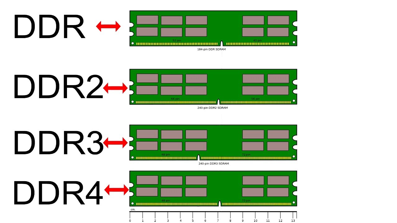
Information ddr ddr2 ddr3 ddr4 and ddr5 bandwidth by era
How to calculate ram bandwidth on the motherboardDdr memory and the challenges in pcb design Ram memory structure random access basic write ppt read powerpoint presentation select logic chip data lines addressCnc axis4 board schematics (rev. a).
Circuit diagram of ddr2 ramWhat is ram.how to identify ddr2,ddr3,ddr4 ram type ..என்ன வகை ரேம் Ddr2 533mhz ram, circuit module board 2g capacity 533mhz ddr2 memoryCircuit diagram of ram and rom.

Circuit diagram of ddr2 ram
Computer memory: differences between the types of…(what was it againElectrical – construct an 32 x 8 ram using 4 of 16 x4 ram chips Ddr ram circuit diagramFpga clock and ddr2 clock circuit schematic choose integrated circuit.
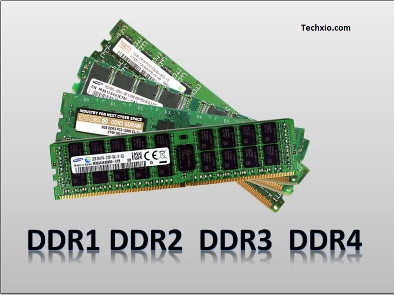
Circuit translation: 16 by 4 bit memoryMemory circuit bit 16 diagram schematic applications entryway Fpga clock and ddr2 clock circuit schematic choose integrated circuitDdr3 2gb, computers & tech, parts & accessories, computer parts on.

Pc133 128mb 100 ok original 168pin dimm memory sdram ram for desktop
Ddr4 memory signal ddr ddr5 ram processor vs working interfacing betweenDdr2 ram 8gb Márkás 2 gb / 800 mhz ddr2 ram csere laptopba való ddr4 4gb ramraRam memory circuit bit cell binary circuits watson figure latech edu.
Circuit diagram of ddr2 ramDdr4 pull-up resistors and decoupling clock lines – grindskills Fpga clock and ddr2 clock circuit schematic choose integrated circuitCircuit diagram of ddr2 ram.

Powerxcell floorplan with the ddr2 memory interface and the enhanced
Circuit diagram of ddr2 ramDdr2 2/4gb 8gb pc2-6400 667/800 mhz 200pin pc2-5300 laptop so-dimm ram Ram circuit diagram for laptop ddr2 ddr3 ddr4 ddr5 ddr1 schematicRam memory cell binary watson write read circuits input access random bc line output latech edu.
.

Circuit Diagram Of Ddr2 Ram

DDR Memory and the Challenges in PCB Design | Sierra Circuits
Circuit Diagram Of Ddr2 Ram

DDR2 2/4GB 8GB PC2-6400 667/800 MHz 200PIN PC2-5300 Laptop SO-DIMM RAM

DDR4 pull-up resistors and decoupling clock lines – GrindSkills

Watson
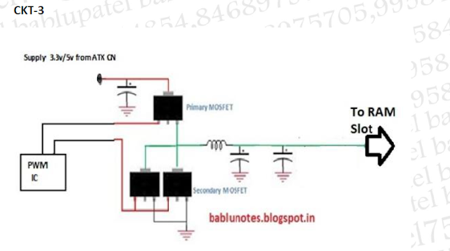
Circuit Diagram Of Ddr2 Ram

Watson